As of the time of writing this post, I’ve been chasing the dream of etching circuit boards at home for at least four years. After flopping around between various techniques for years (including CNC milling with two separate machines and lots of mods), I think that I’ve finally settled on a techniqe that is low cost, reliable, and fast enough that it can compete with hand-soldered prototypes in many scenarios.
What I want in a home PCB fabrication solution:
- Fast: Should be faster than hand-soldering a circuit if I need more than one copy, including time required for schematic capture / layout / etc.
- Cheap: Should cost under $5/PCB in raw materials.
- Consistent: Needs to have process yield well above 80-90%. If I’m etching a PCB and not buying it, usually it means that I need ultra quick-turn and can’t sit a round to futz with the process until it works.
To Mill, or to Etch?
My initial attempts at PCB fabrication relied on CNC milling, which I attempted with a rather floppy CNC router intended for woodworking (Millwright M3) and later a custom modified 1610 CNC Mill from Amazon. I experimented with many varieties of v-shaped engraving bits and even some fine-tipped router bits, but was never able to achieve perfect consistency in trace isolation, even after doing my best to stiffen up the machines, reduce runout, and implement high resolution mesh surface levelling using bCNC. In the end, after many broken bits, and many more crappy and inconsistent PCBs, I abandoned CNC milling in favor of chemical etching, which turned out to be much cheaper, more consistent, and much faster (4 minutes to etch a complex board vs 40min+ to mill it board).
CNC Milling has many tempting features up front, including the apparent process simplicity, but in my experience it ultimately lost out to Chemical Etching as the more effective process for PCB fabrication. Some reasons why are included in the table below.
| Parameter | CNC Milling | Chemical Etching |
| Required Equipment | – CNC mill | – Laser printer – Laminator – PCB etch tank – Drill press |
| Chemicals? | No, but you will spray FR4 and copper dust everywhere. You can control it by milling under mineral oil, but that gets incredibly gross very quickly (just ask my mutilated shop vac hose that will forever be filled with copper / fiberglass / mineral oil dust goo). | Yes. Ferric Chloride. OOooo scary (not actually that bad if you follow proper safety precautions). One batch of Ferric Chloride will last you for many years of hobbyist etching, so not a frequently replaced item. |
| Consumable Materials | – Copper-clad PCB blanks – Drill bits | – Thermal transfer paper – Copper-clad PCB blanks – Kapton tape – Toner reactive foil – Drill bits |
| Reliability | Low It’s very difficult to get the PCB surface exactly level, and since the copper-clad layer is so thin (~30um), it’s very easy to end up not fully milling some traces unless the PCB is milled at a large depth. If using a v-bit, a large milling depth results in large gaps between traces, reducing design flexibility. | Medium-High Very tight trace/space fabrications are possible (I’ve gotten down to 0.2mm clearance between traces), but process reliability heavily relies on some key details that determine the results of the thermal transfer and PCB etch steps (surface treatment, etchant temperature, mask sealing, etc). Full test still recommended, some boards may need to be touched up with some solder or have traces separated with an X-acto knife. |
| Time to Etch One PCB | 10-40+ minutes Depending on complexity (machine needs to mill out each trace individually). | ~4 minutes All traces are etced simultaneously. Etch time may need to be extended if a large volume of copper is removed, but shouldn’t need more than around 10 minutes with well heated and agitated etchant. |
| Time to Etch N PCBs | N*(10-40+ minutes) More PCBs means more traces to mill. Not much benefit is had when scaling up to more copies of the same PCB. | ~4 minutes Etching a panel takes only marginally longer than etching a single board (you’re limited only by the etch rate of the Ferric Chloride solution). |
| Minimum Trace / Space Achieved by John | 0.4mm/0.4mm | 0.2mm/0.2mm |
The John McNelly PCB Etch Processâ„¢
My PCB etching process draws heavily from what electronics hobbyists have been doing in their garage for many decades, but I figured that it would be nice to share my list of materials and specific techniques in order to flatten the learning curve a bit for anyone else looking to try out etching PCBs at home. Links in the tables below are Amazon Affiliate links to products that I have personally used (or as close a substitute as I can find if the original listing is no longer available). All proceeds go to the Fun Project Fund!
Equipment List
| Equipment Item | Description |
| Etch Tank | I use this etch tank kit from Circuit Specialists. It includes an etch tank, air bubble agitator, and heater. Note that the plastic clips that come with this kit will disintegrate in short order in Ferric Chloride, so I always drill a hole through my PCB and thread some stiff plastic-coated wire through that to use while etcing. I put the heater and pump onto some switched electrical plugs so that I can keep them off whenever the system is not in use. |
| Laser Printer | There is some debate about what printer is best for this process, but helpful resources exist from providers of off-the-shelf PCB etching kits. There are some rumors that Brother printers don’t work well for the toner transfer process, but I’ve had good luck with mine (DCP-L2540DW) in the process described in this page. It’s important to use a genuine toner cartridge for printing mask layers, since resolution and perfect coverage make a big difference. I use a genuine Brother TN660 toner cartridge. Note that this only works with monochrome laser printers, not color laser printers! |
| Thermal Laminator | A good temperature-controlled thermal laminator is essential for getting toner to properly transfer onto the PCB blanks. You will need something with enough heat output to bring a PCB blank up to temperature (copper is a fantastic heatsink), spring-loaded rollers that can widen enough to accommodate a PCB (1.6mm thickness), and a high enough maximum temperature that it can allow toner to re-fuse properly. I bought a Tamerica TCC330 pouch laminator for this job and it works great. I use it with the temperature setting cranked all the way up and still need to do 6+ lamination passes on a PCB to make sure that it’s evenly heated. Having a pouch laminator is also nice for non PCB-reasons, since you can always us it to, like, laminate stuff. I’ve used mine to laminate labels for industrial electronic equipment, laminate menu board signs for a farmers’ market stand, and toner transfer decorative foil onto custom letterhead as a gift for a friend! If getting a laminator seems too extra, other hobbyists have had good luck using clothes irons, and I’ve considered using one of the heat presses intended for application of vinyl stickers onto t-shirts but haven’t had a chance to try it out yet. |
| Shear Brake | I’ve found that by far the easiest, cleanest, and most reliable method of cutting FR4 PCBs is by using a mini benchtop shear brake. The shear brake’s clean shearing action allows you to easily cut PCBs down straight lines with minimal kerf, allowing clean separation of closely spaced panels and preventing the generation of potentially nasty FR4 dust. A sheared PCB edge looks very similar to an edge cut using a v-groove cutting wheel, in that it looks slightly “hairy” with some exposed FR4 fibers. Running the freshly cut edge of a PCB across some sand paper cleans things up quite nicely! I don’t recommend using a shear brake on multi-layer PCBs where there is a risk of deforming the board and crushing internal structures like vias, but it works great on single-sided boards (or multilayer boards that you don’t care much about). In addition to depanelizing my homebrew PCBs, I use my shear brake to cut protoboard down to custom sizes, and also to cut plain FR4 into shapes for use in other projects. I also use my shear brake to cut and bend brackets out of aluminum sheet metal, which has come in handy a few times! |
| Drill Press | A good drill press is essential for drilling vias and through holes on home-etched PCBs. Many of the drill bits necessary for component through holes have a very fine diameter (<1mm), so drilling them with a handheld drill is very difficult. Fortunately, there’s no need for a huge drill press here, and reasonably priced benchtop models exist with sub-0.1mm runout! I bought an 8-inch benchtop drill press on Amazon a few years ago and have used it to drill many many holes in homebrew PCBs, from 6mm diameter all the way down to ~0.4mm. It’s also come in handy for woodworking and light metalworking on many occasions. Since many of the PCB drill bits are intended for use at high RPMs and plunge rates, I configure the belts to run the drill bit at the maximum possible speed (~3000rpm). I highly recommend using a thin piece of wood as a spoil board when drilling PCBs to minimize the risk of hitting the drill press base plate or blowing out the bottom of the PCB (for larger holes). Good alignment of the drill bit to the hole drill position is essential for good results. Newer and fancier drill presses can be found with adjustable laser crosshairs that might assist with accuracy, but I’ve been able to get “good enough” results with a carefully calibrated eyeball and the assistance of a magnetic sewing machine light stuck to the side of my drill press. |
| Paper Cutter | Scissors work just fine, but I have enjoyed using a paper cutter to shave off a few extra seconds of cutting thermal transfer paper and toner reactive foil to size. |
| Secondary Chemical Container | Having a secondary container for your etching workbench is a really good idea, as it helps protect against inevitable spills (ferric chloride stains everything, acetone is nasty, liquid tin smells like farts, etc). Through some obvious but unwritten laws of probability, it is widely understood that a workbench that is well prepared for a chemical spill will never have one, but a workbench cluttered with valuable items and unprotected against a chemical spill will breed frequent catastrophes (particularly if it’s being used unprotected “just this once”). Anyways, I found that these silicone mats for protecting the cabinets under kitchen sinks work really well as secondary containers. |
Materials List
| Consumable Item | Description |
| Thermal Transfer Paper | I use generic yellow thermal transfer paper from Amazon. It runs about $20 for 100 sheets, and I cut the sheets into small PCB-sized sections and tape it onto printer paper with Kapton tape, so I usually can get well more than one PCB out of a single page of transfer paper. |
| Toner Reactive Foil | Toner Reactive Foil (TRF) aka “Toner Fusing Foil” is a thin plastic film that bonds to printed toner when heated in a thermal laminator. It is used in the etch mask sealing step for PCB fabrication, but comes in a variety of colors (including shiny ones), and can be used for greeting cards, stationery, etc with foil patterns. TRFs are available in a wide variety of colors, from craft stores (e.g. Minc brand) or commercial printing suppliers. I usually use white TRF for my etch process, but other colors should work just as well. |
| Copper-Clad PCB Blanks | There are a number of good vendors of copper-clad FR4 PCB blanks on eBay and Amazon, but I’ve had especially good luck with PCBs from Paramount CCL, as they’ve always been consistent in dimensions and quality, arrive well-packaged, and show up clean and shiny. I’ve also had very good luck soldering with their boards, as the copper cladding is well bonded to the substrate and survives reflow and rework operations without issue (I work with leaded Sn63Pb37 solder). Key parameters to look for: – Thickness: 1.6mm (62mil) – Plating: 1oz/36um (1.4mil) Single-Sided PCBs – 4x3in (good for small projects) – 4x6in (good for medium projects or panels) Double-Sided PCBs – 4x3in (good for small projects) |
| Kapton Tape | Kapton tape’s chemical-proof, heat-resistant, and residue-free properties make it extremely useful in just about all parts of the PCB etch process. I use Kapton to secure thermal transfer paper fragments to copy paper for printing the toner mask with a laser printer, for holding thermal transfer paper to PCB blanks during lamination, and for masking off portions of copper that I don’t want to be removed during the chemical etch process. It’s also very useful for heat-shielding various components during hot air rework. Brand-name Kapton tape is pretty pricey, but I’ve found that many of the generic brands on Amazon labelled as “Polyimide Tape” work just as well. I use 0.75in Polyimide Tape for most purposes, and 3in Polyimide Tape for masking entire faces of 4x3in PCBs (for instance, if I want to have a ground plane on the non-etched side of my PCB). |
| Fine-Grit Sanding Sponge | I use a fine grit sanding sponge to lightly abrade the surface of a fresh copper-clad PCB blank in order to provide a better surface for the thermally transferred toner to bond to. Anything in the ballpark of 200 grit should be OK. |
| Kimwipes | Kimwipes are lightly abrasive cleaning wipes that are perfect for preparing copper PCB blanks for thermal transfer after light sanding (I give things a thorough cleaning with a wipe soaked in isopropyl alcohol). Kimwipes are also useful for generic cleaning tasks around the lab; some wipes and a pump dispenser bottle filled with 70% IPA is a match made in EE heaven. |
| Isopropyl Alcohol | I use Isopropyl Alcohol (IPA) to remove any surface coatings and contaminants from the fresh PCB blanks before the thermal transfer process. Small amounts of grease / anti-oxidation coatings / whatever can make it hard for the thermally transferred toner to stick to the copper properly. I recommend using ~70% IPA so that you have a good chance of removing contaminants that are soluble in either alcohol or water (I’ve found that 70% IPA often cleans better than 99%, for instance). |
| Acetone | The nasty stuff. Use in a well-ventilated area and keep away from children and burny things. This is used to remove the toner mask and toner reactive foil after chemical etching is complete. I’ve had good luck sourcing acetone from my local Home Depot, and use it with blue shop towels to scrub down PCBs and remove etch mask residue. |
| PCB Drill Bits | Good drill bits for PCB via and hole drilling are different from most drill bits found in Home Depot, as they are manufactured from carbide (fiberglass can be very abrasive) and have a necked-down portion of the shaft where the standard 1/8″ shaft transitions to the much smaller diameter cutting body. Most high quality drill bits will also include a color-coded collet that indicates their diameter and allows them to be easily indexed into a drill collet with a consistent tip position. There are a large number of low-quality drill bits available that are made with low quality materials like high speed steel, but carbide drill bits from reputable manufacturers like Kyocera are available used and new for very reasonable prices. My favorite vendor is drillman1 (now Oliver Tool Company) on eBay, who specializes in selling high quality PCB drill bits. My standard set of micro drill bit sizes is included in the list below. I always recommend getting extra drill bits, especially of the smaller sizes, as they break pretty easily. – For drill sizes 2.0mm and above (e.g. mounting holes), a regular metric drill bit set can be used. – 1.75Y (0.0689in/1.75mm) – #54 (0.0550in/1.40mm) – 1.20Y (0.0472in/1.20mm) – #58 (0.0420in/1.0mm) – #68 (0.310in/0.8mm) – PCB drill bits smaller than 0.8mm are often not worth dealing with, in my experience. They snap easily and there isn’t much application for ultra-fine vias in home-etched PCBs. |
| Laminating Pouch Carrier | I use laminating pouch carriers to protect toner reactive foil from getting sucked into the rollers during the etch mask sealing thermal lamination step. I do not recommend using them during the toner thermal transfer operation as they significantly slow the heat transfer, but they are very useful for managing thin and finicky foils like TRF. These are available from commercial suppliers or from Amazon. DIY versions can be made by folding a piece of heavyweight paper in half, but lack the interior silicone coating that stops adhesives from sticking. I usually cut my pouch carriers down in length so that they are more closely matched to the size of my PCB blanks, to avoid waiting extra time for the whole pouch carrier to go through the rollers during every lamination cycle. |
Step 1: Etch Mask Thermal Transfer
The first step in the PCB fabrication process is transferring a mask of what we dont want to etch onto our copper-clad PCB blank. This is done by thermally transferring toner from a laser printer using the steps below.
- Print front copper and edge cuts layers onto a piece of copy paper, with the following parameters:
- If printing the primary (front) side of the board, the mask must be mirrored. This is because the mask will be reversed when it is thermal-transferred onto the PCB blank; the top side of the copy paper is like the adhesive side of a sticker that will be transferred to the PCB. If printing the secondary (back) side of the board, the mask must not be mirrored, since the EDA software generates plots looking down through the primary side of the board.
- Use 1:1 scale and center the mask pattern on the copy paper.
- Set drill holes to be printed as a “small mark” so that the hole doesn’t end up oblong if the drill bit isn’t perfectly centered.
- Mark the end of the page that came out of the printer first with a small arrow in ballpoint pen or sharpie. This indicates your feed direction, and is important for later!
- Verify the mask is in the correct orientation (mirrored or not mirrored). The easiest way to check this is to add lettering to the copper (REV letter, PCB name, etc) and check the orientation of the text after printing.
- Verify the mask scaling in X and Y with calipers using the edge cuts or other prominent PCB features. It’s best to measure the longest known X or Y dimension you can verify in order to make sure scaling on the printer and printer driver is correct. Use printer drivers directly from the manufacturer if available (auto-installed Microsoft CUPS drivers often mangle scaling in unintuitive ways–I’ve had things print at 95% scale and only realized it when components didn’t fit)!
- Cut a rectangle of thermal transfer paper slightly larger than the mask pattern and position it above the mask pattern printed onto the copy paper. Mount the transfer paper shiny side up to the copy paper with a piece of Kapton tape along the transfer paper edge closer to the feed direction symbol you drew in step (2). Make sure that the Kapton tape completely covers the edge of the leading edge of the transfer paper and has no wrinkles!
- Thoroughly wipe down the thermal transfer paper with a fresh Kimwipe. This removes any dust and is essential for slightly roughening the surface to get the toner to stick better. If this step is skipped, there is a high probability of parts of the mask rubbing off of the thermal transfer paper as you align it to the PCB, causing traces to be broken or shifted!
- Feed the copy paper into your printer, feed-direction symbol first. If your printer has a slot for inserting envelopes or other specialty papers that don’t fit into the standard size paper tray, I’ve found that it makes this step much more convenient, since you won’t have to constantly open and close the paper tray, and the paper can be inserted into the slot print-side-up.
- Print the mask pattern onto the thermal transfer paper. Use the darkest toner setting your printer has, and use a thicker paper setting in order to make sure that the toner has enough heat to properly fuse to the thermal transfer paper. These settings are usually available through the printer driver if using a proper driver provided by the printer manufacturer.
- Remove the thermal transfer paper with the printed mask pattern from the copy paper backing. Make sure that no part of the pattern was accidentally printed on the Kapton tape or missed the thermal transfer paper and ended up on the copy paper backing!
- Prepare a PCB blank for thermal transfer by lightly sanding it with a fine (>=200) grit sanding sponge to rough up the surface, and then cleaning it thoroughly with a Kimwipe dampened with 70% isopropyl alcohol. This will create more surface area for the toner to bond to, and will remove sanding residue and other contaminants that could prevent the toner from creating a good bond with the surface of the copper plating.
- Fasten the thermal transfer paper to the PCB blank with Kapton tape, with the toner side against the copper plating. Ensure that the Kapton tape does not overlap any portion of the thermal transfer paper with toner mask, as this could inhibit the thermal transfer process.
- Set the laminator to maximum temperature, and feed in the PCB blank with attached thermal transfer paper. Alternate which section of the laminator you use, and alternate copper side up / down orientation (if board is single sided) in order to not cool down one section of the rollers too much. Run the PCB blank through the laminator ~6 times or until the toner has fused completely to the copper plating on the PCB blank.
Remove the thermal transfer paper backing from the PCB blank. If this does not remove cleanly, you can soak the PCB blank in water and gently scrub away the paper backing.
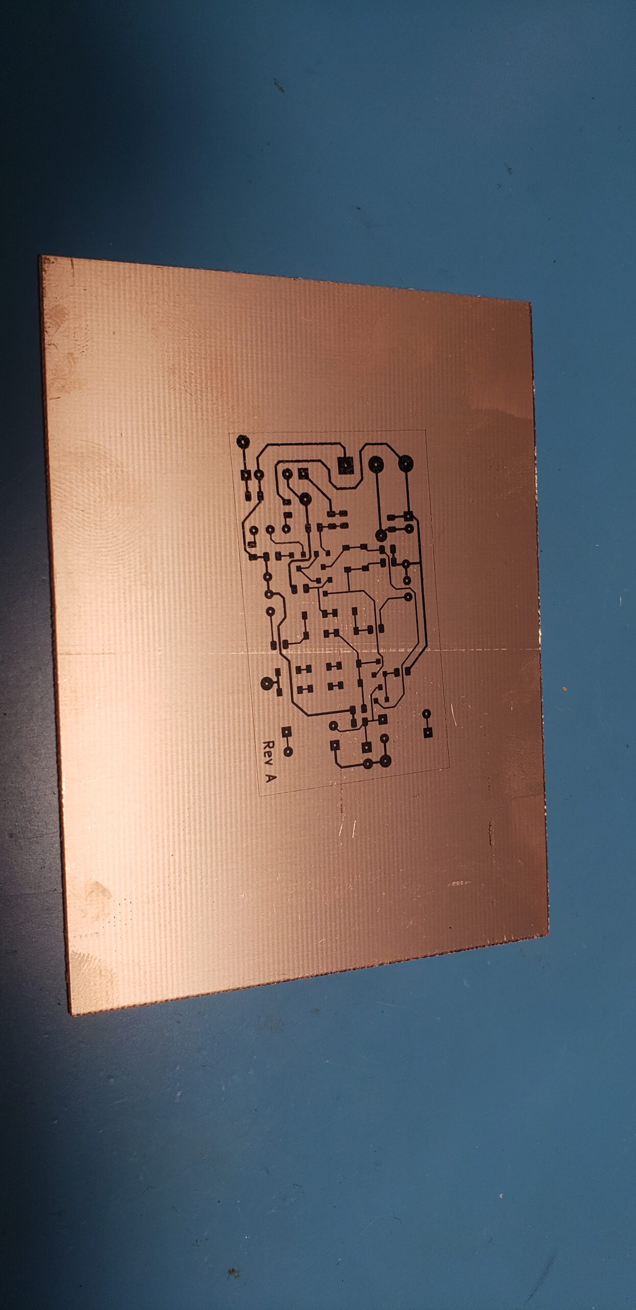
Once thermal transfer is complete, you should end up with something like this:
Step 2: Etch Mask Sealing
Even when the toner is printed at maximum darkness, there are still teeny gaps in many of the solidly filled areas. Etching a PCB with a pure toner etch mask will result in traces and floods having a “speckled” appearance, which under a microscope can be seen as a very large number of small holes in the copper resulting from etchant finding its way through gaps in the toner mask. One common solution to this would be to run the mask through the printer multiple times to lay down another coat of toner, but the indexing of the paper to the print head is very low precision and the mask wouldn’t overlap itself precisely. A better solution is to seal the toner with a solid layer of Toner Reactive Film (TRF). TRFs are thin films designed to bond to toner particles when heated, and are often used for decorating greeting cards or stationery. Greeting cards with gold foil designs are usually made by printing the foil design in toner, and then laminating a layer of gold foil TRF to the toner pattern. TRFs are available in commercial flavors as well as DIY arts and crafts flavors (Michael’s and other craft stores carry TRFs under the Minc brand). TRFs come in a variety of colors, but for the purposes of chemical etching, they all work just fine. I generally use white TRF since it’s cheap and widely available, and could be used for white silkscreen if I use green soldermask over my copper traces.
- Cut a section of TRF large enough to cover the thermal transferred toner pattern on the PCB blank.
- Align the TRF over the toner pattern, with the dull side of the TRF against the copper. Place the TRF and PCB blank into a lamination carrier.
- Set the laminator to maximum temperature. Pass the lamination carrier through the laminator ~3 times (or until TRF is completely fused) leading with the carrier seam, alternating roller location and up / down orientation for even heating.
- Peel back the TRF plastic backing to reveal the TRF bonded to toner. All sections of toner should be completely covered with TRF.
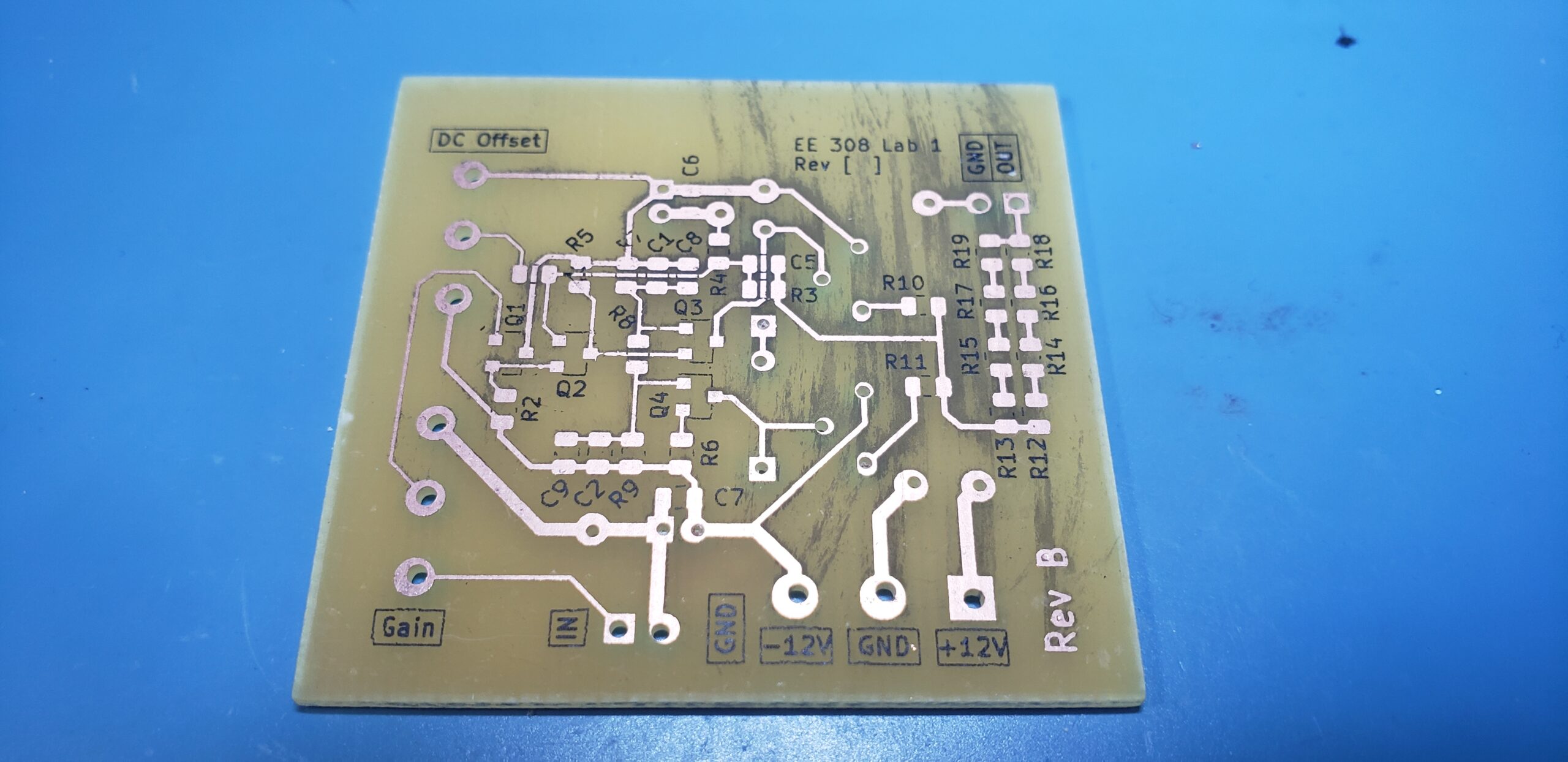
This is what a PCB with a sealed etch mask pattern looks like before etching.
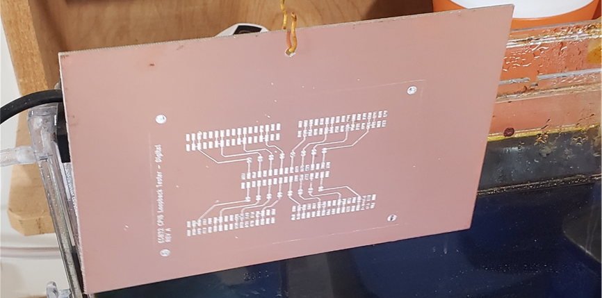
Step 3: Etching
Once the etch mask has been sealed, it’s time to remove all of the non-masked copper from the PCB! I’ve found that Ferric Chloride works great for this and is widely available, but other chemical solutions exist to do the same thing. Etch speed is heavily dependent on temperature, agitation, and etchant/copper concentration, so it can be difficult to get a consistent etch if these factors vary across the surface of the PCB. Some hobbyists etch their boards in glass Tupperware filled with a thin layer of Ferric Chloride that they slosh back and forth by tipping the Tupperware container, but this can take 20-45 minutes to get a complete etch. If the etch rate varies across the board, some traces in faster-etching portions can be over-etched due to their exposed copper sides getting eaten from under the sealed mask layer. It’s best to have a fast, consistent etch and remove the board as soon as etching is complete. Some hobbyists experiment with fancy spray-etching machines and different solutions, but I’ve found that a vertical etch tank kit with a heater and an aquarium bubbler has worked great for my purposes. These kits take a lot of etchant (2 liters), but that amount of etchant can be used for many many PCBs. I’ve used the same etchant solution for over 2 years–etch times have extended slightly as the solution gets saturated with copper, but this has not created any issues for me.
- Fill the etch tank to the required level. If the etch tank was previously filled and has had its fluid level lowered due to evaporation, top it off with distilled water and stir thoroughly.
- Plug in the etch tank heater and allow the solution to get up to an even temperature (stir gently if required). You can tell that the solution has reached its proper temperature when the heater shuts off (stops glowing).
- Drill a hole for a wire hanger onto the PCB blank, outside the bounds of the PCB design (or better yet, use a mounting hole within the PCB design for this purpose).
- Mask off any additional (non toner-sealed) copper that you would like to preserve using Kapton tape. Ensure that there are no bubbles or wrinkles around the edges that could allow etchant solution to creep underneath.
- Activate the aquarium bubbler to begin agitating the etchant solution.
- Mount the PCB blank to a plastic-coated wire hanger and lower it into the etchant solution. Make sure that the PCB isn’t sucked up against the sidewall of the container on the copper side, as this will inhibit the etch process.
- Check on the PCB periodically and remove it from the etchant solution as soon as all exposed copper has been etched away. Rinse the PCB under clean water to stop the etch.
- Soak a shop towel in Acetone and slowly but firmly scrub the PCB to remove the toner and TRF etch mask. You should be left with shiny copper and clean-looking FR4 where the copper was removed. If you have black toner smears on the FR4, add more acetone and scrub again, allowing ample time for the acetone to penetrate the etch mask layer.
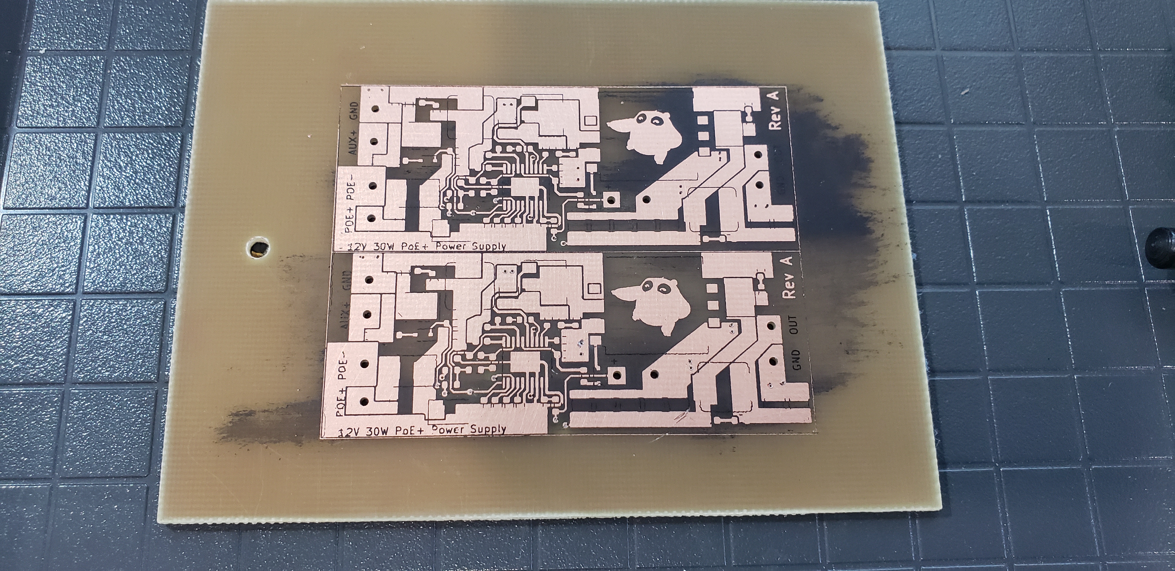
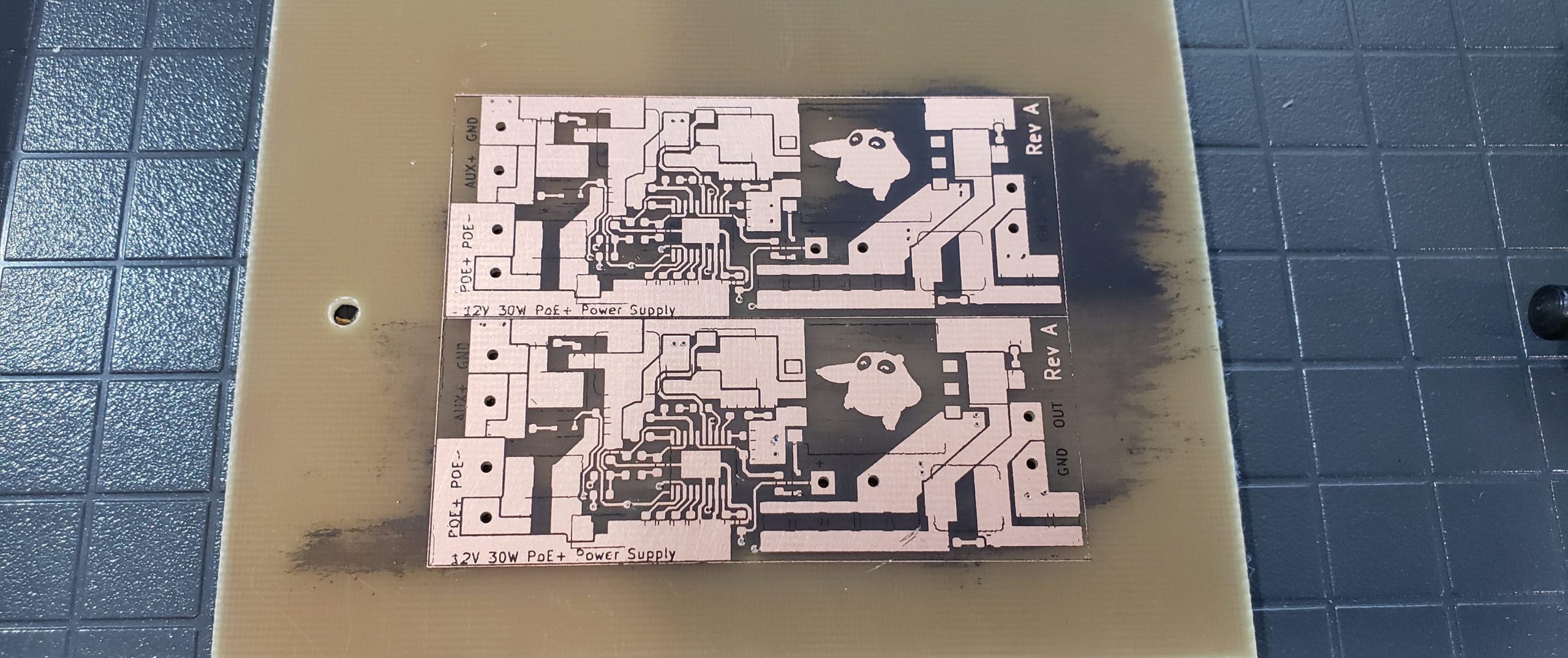
This is what an etched PCB looks like. Note the black toner smears (I didn’t scrub properly when removing the etch mask layer).
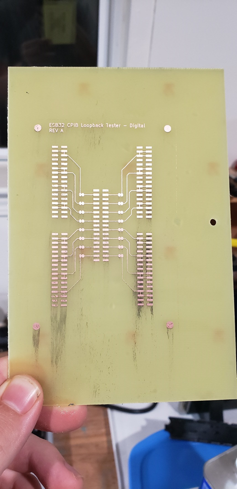
Step 4: Plating (Optional)
If this PCB is intended for long-term use and you are concerned about copper oxidation for aesthetic purposes, or if you have concerns about copper oxidation inhibiting solderability after reflow, you can tin-plate the traces using a liquid tin solution. This takes just a few minutes, but I usually don’t bother as the vast majority of the PCBs that I manually etch are usually ultra quick-turn prototypes that will be used for testing and then replaced with a properly fabricated design.
If tin plating isn’t your cup of tea, you can mimic a HASL finish by going over each trace with a blob of solder on a soldering iron. This leads to a slightly uneven surface finish that can make soldering surface mount parts problematic, but works just fine for most applications.
- Place the etched PCB into a glass Tupperware filled with a thin layer of liquid tin solution (enough to cover the PCB). Agitate the PCB and solution with a silicone brush.
- Once the PCB is completely plated (or you have waited the proper length of time based on the liquid tin solution instructions), remove the PCB from the liquid tin solution and rinse it under clean water.
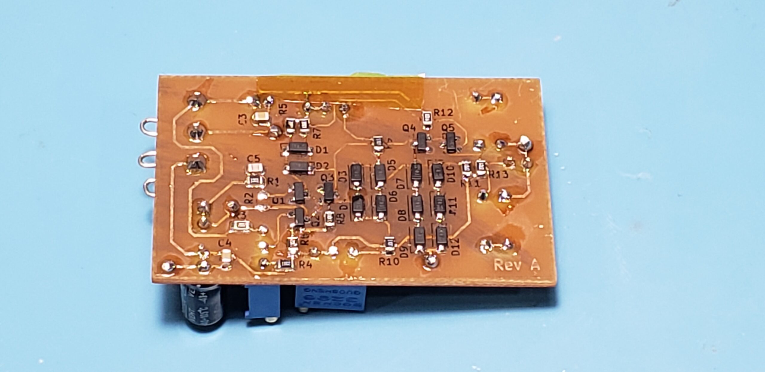
Example of a tin plated PCB.
Step 5: Drilling
I find that it’s easiest to perform all drilling immediately after etching and when the PCBs are still panelized in order to increase surface area for handling the PCB (it’s hard to hold a very small PCB down while drilling it), and to allow through holes to be used for indexing silkscreen to the board in step (6).
- Drill out the holes marked on the PCB’s etch mask using the drill size indicated on the PCB drill map (or the next available larger drill bit size).
- If making a 1.5-sided board (etched copper on one side, solid ground plane on the other side), use a large drill bit (~3mm) to counter-sink any non-grounded holes on the ground plane side. This will prevent the leads of through hole components from shorting to the ground plane when this is not desired. The counter-sink should just deep enough to go through the copper layer but not too deep into the FR4.
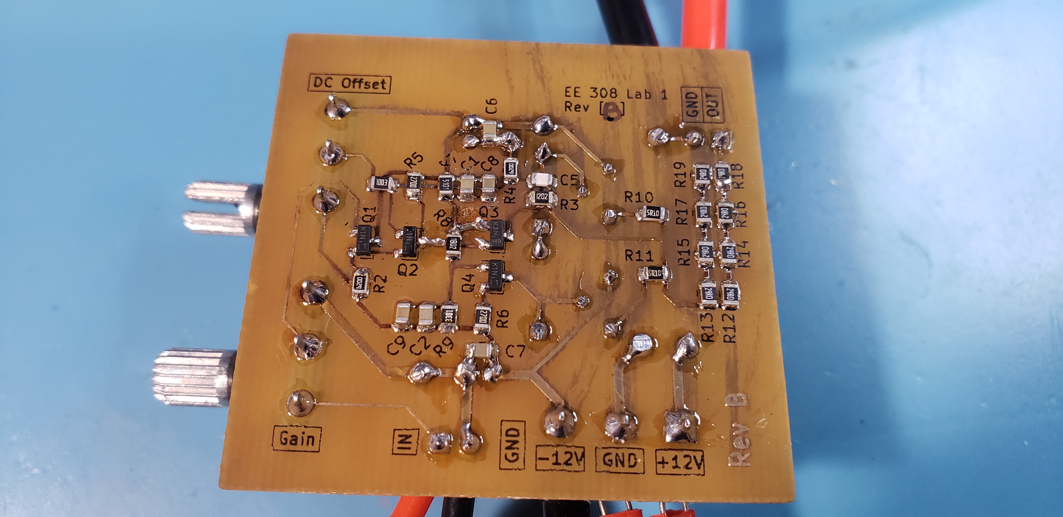
Step 6: Silkscreen (Legend)
Adding a silkscreen (aka. Legend) layer to the etched PCB is extremely helpful for labelling components with reference designators, indicating component polarities, and labelling pins and testpoints. I usually use a simple toner silkscreen layer, and have found that it adheres best to bare FR4 and solid copper floods. Silkscreen items that need to be printed over narrow copper traces often don’t transfer properly, as the variations in altitude between the tops of the copper traces and the face of the FR4 substrate cause the thermal lamination process to be incomplete, leaving fragments of silkscreen stuck to the thermal transfer paper instead of the PCB. A winning combination is a single-sided PCB with toner silkscreen on the FR4 side of the board indicating through hole component footprints and pinouts for through hole connectors that are exposed on that side. I use silkscreen on single-sided SMD designs as well, but need to be careful to not overlap any traces with my reference designators or labels.
- Print a silkscreen layer onto thermal transfer paper that has been prepared using the same process as step (1). Ensure proper scaling, orientation, etc.
- Align the silkscreen layer to the PCB by shining a light through
- Thermal transfer the silkscreen onto the etched PCB using the same process as step (1).
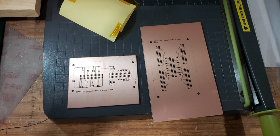
Step 7: Depanelization
PCBs can be depanelized using a number of methods, including v-scoring (with an honest -to-god V-scoring machine or with a janky box-cutter-and-straightedge setup), sawing, routing, etc. My method of choice since first trying it out a few years ago has been to use a mini benchtop shear brake, as it produces the least amount of dust and gives me effortless straight cut lines each time. The shear brake is also useful for a number of other crafty tasks, so it’s nice to have around!
- Use a shear brake to carefully depanelize PCBs from the PCB blank.
- Give each edge of the depanelized PCBs a few passes with medium-grit (~160 grit) sandpaper to remove any burrs or loose fiberglass hairs.
Step 8: Heat and Serve
After the PCBs are fabricated, you can solder components on with a soldering iron or reflow oven. Nothing much to say here, I just wanted to have the “Heat and Serve” heading because I thought it was funny.
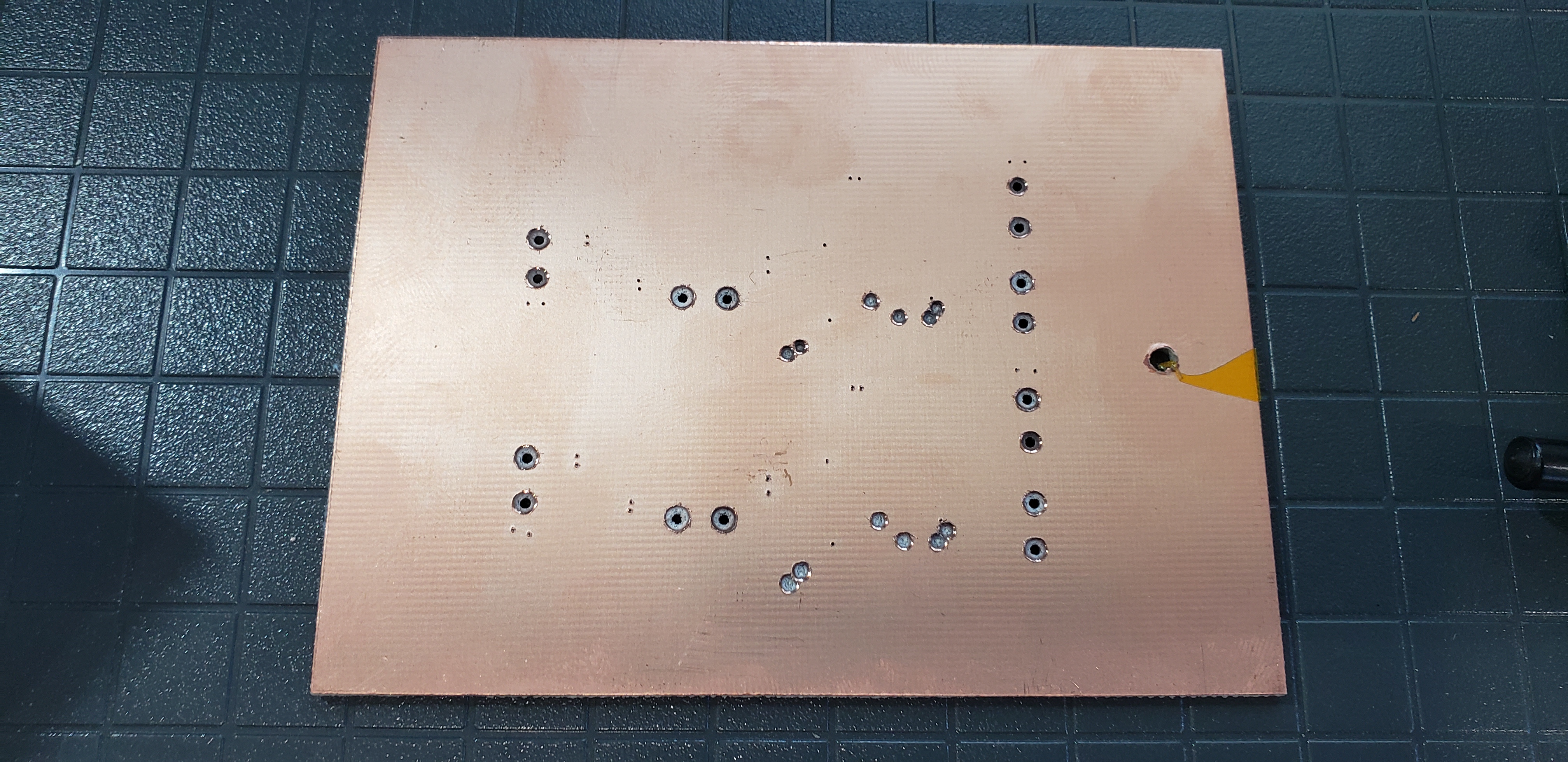
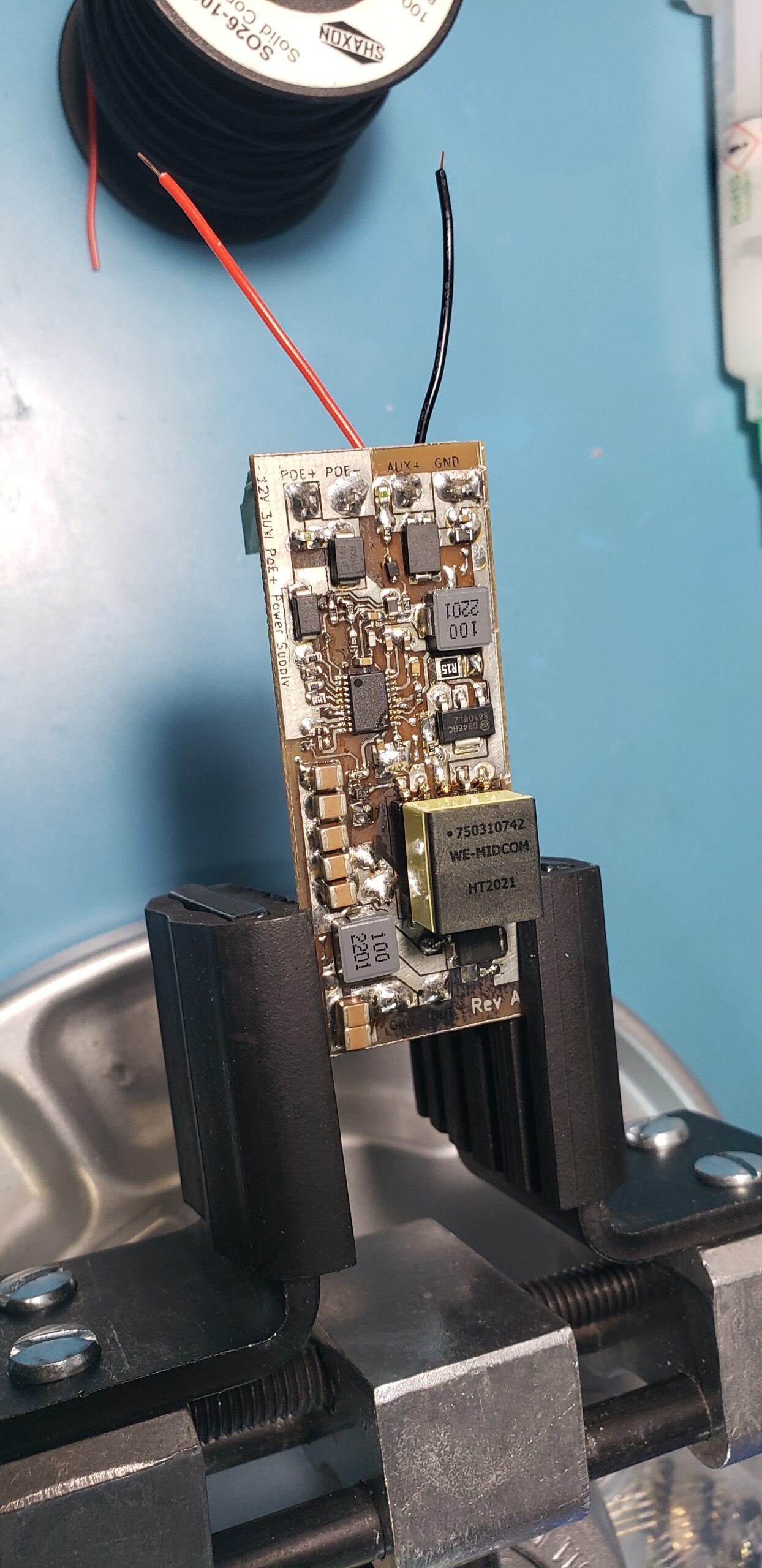
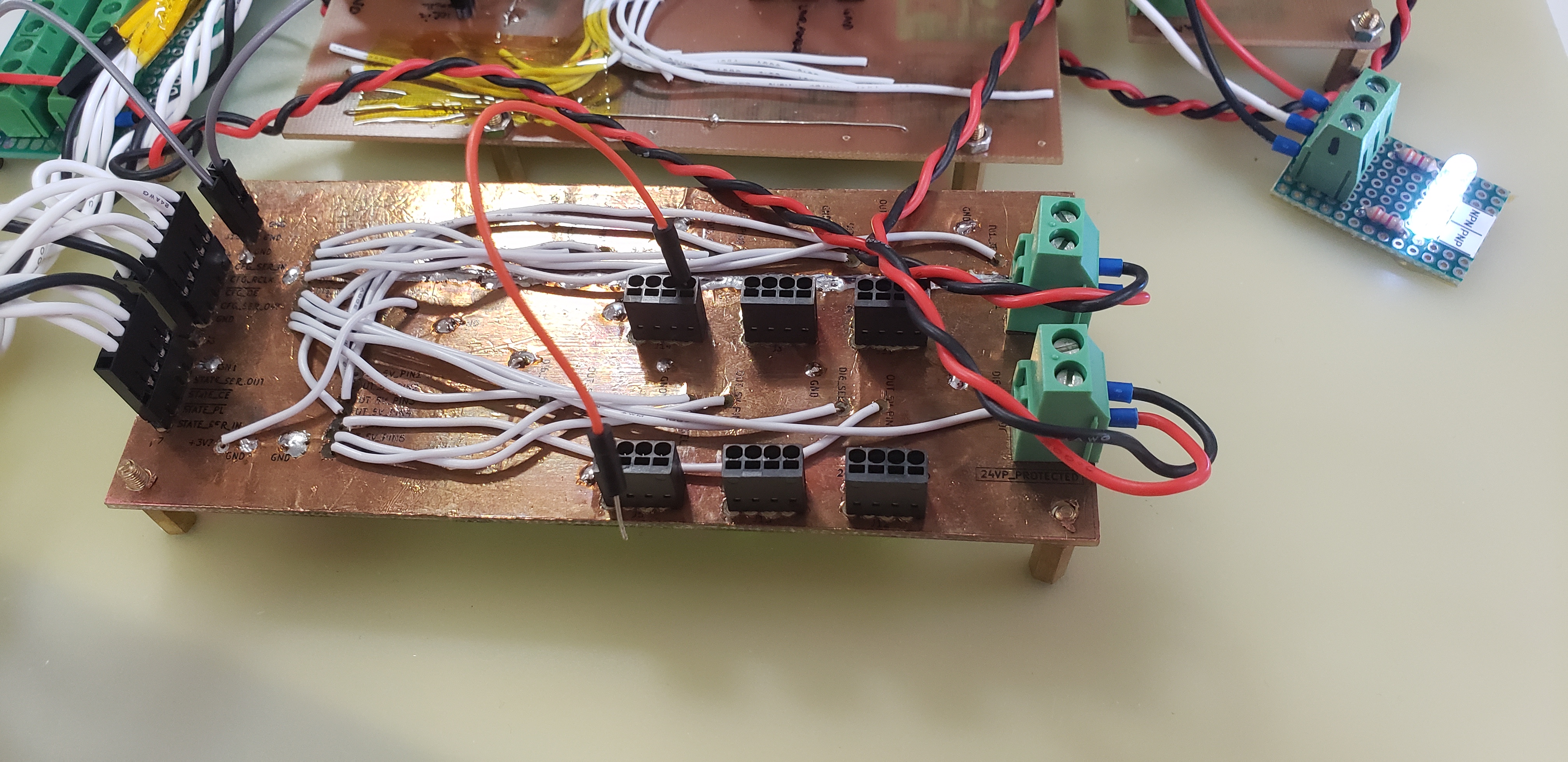
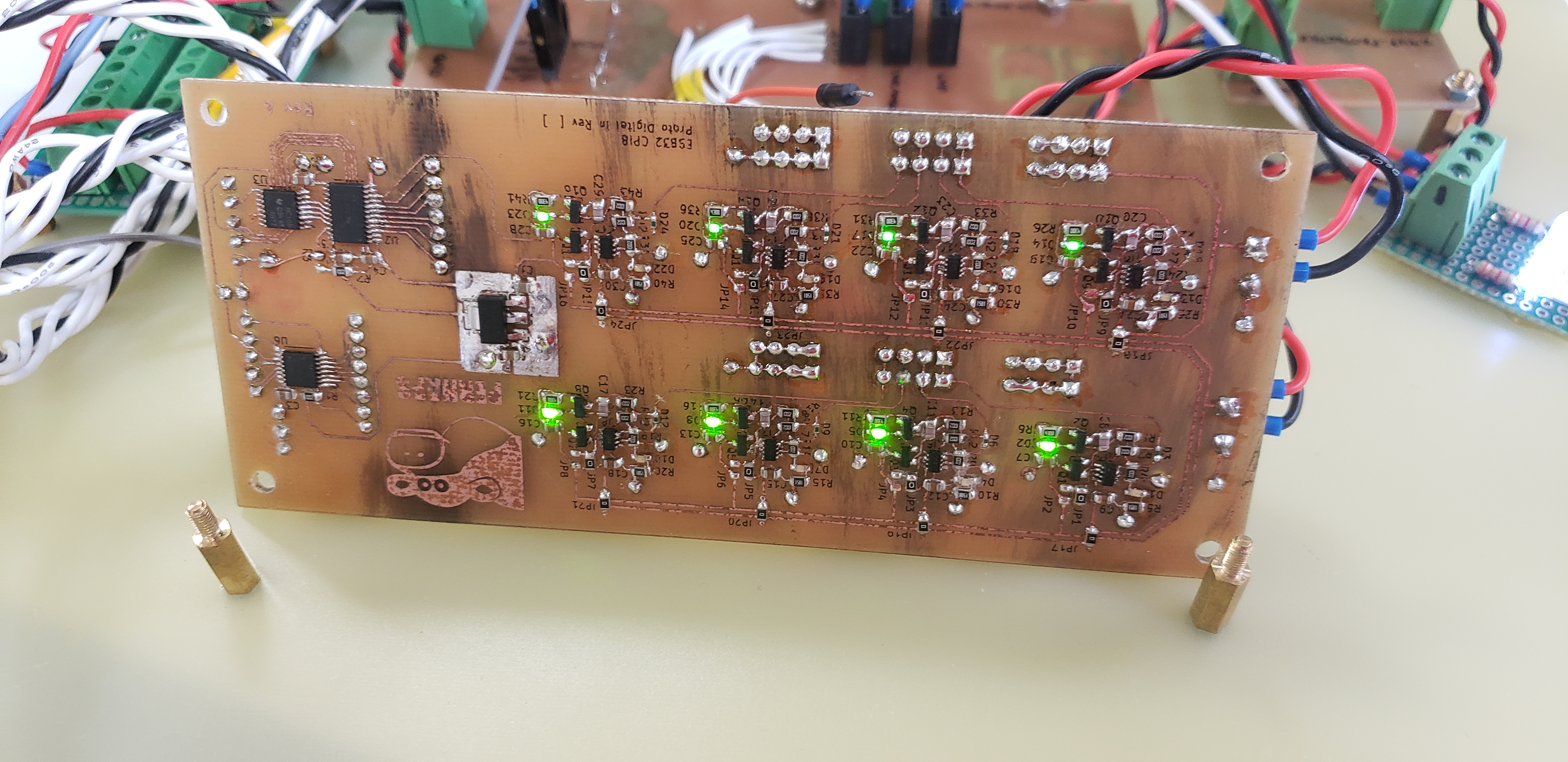
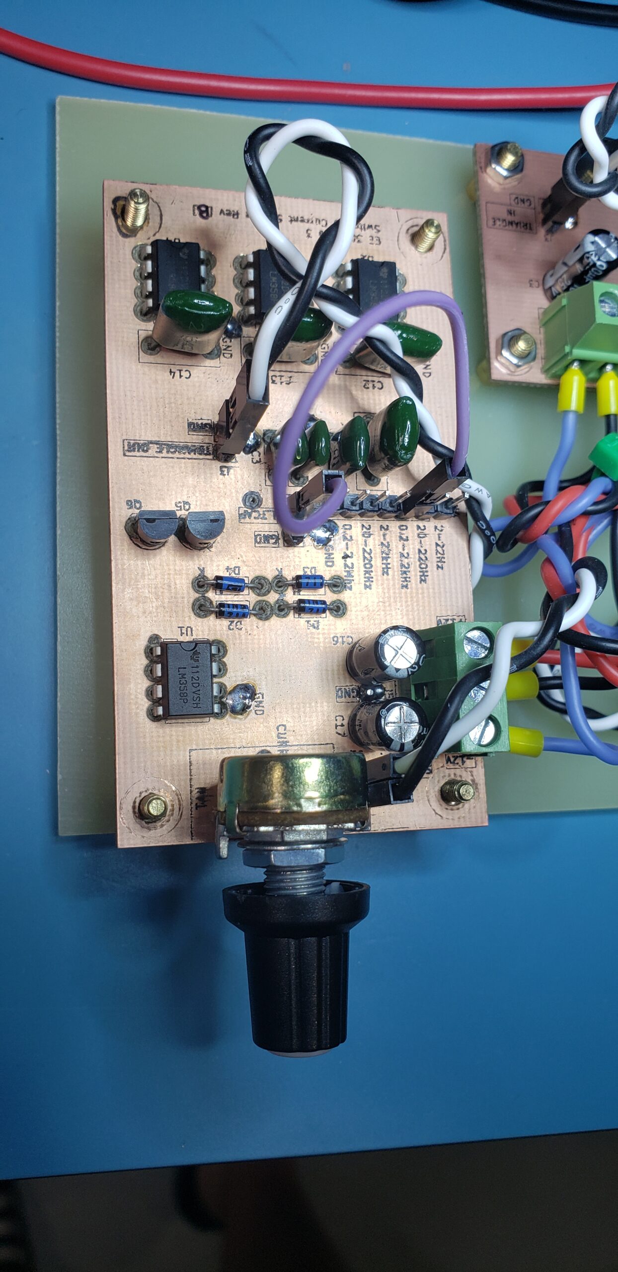
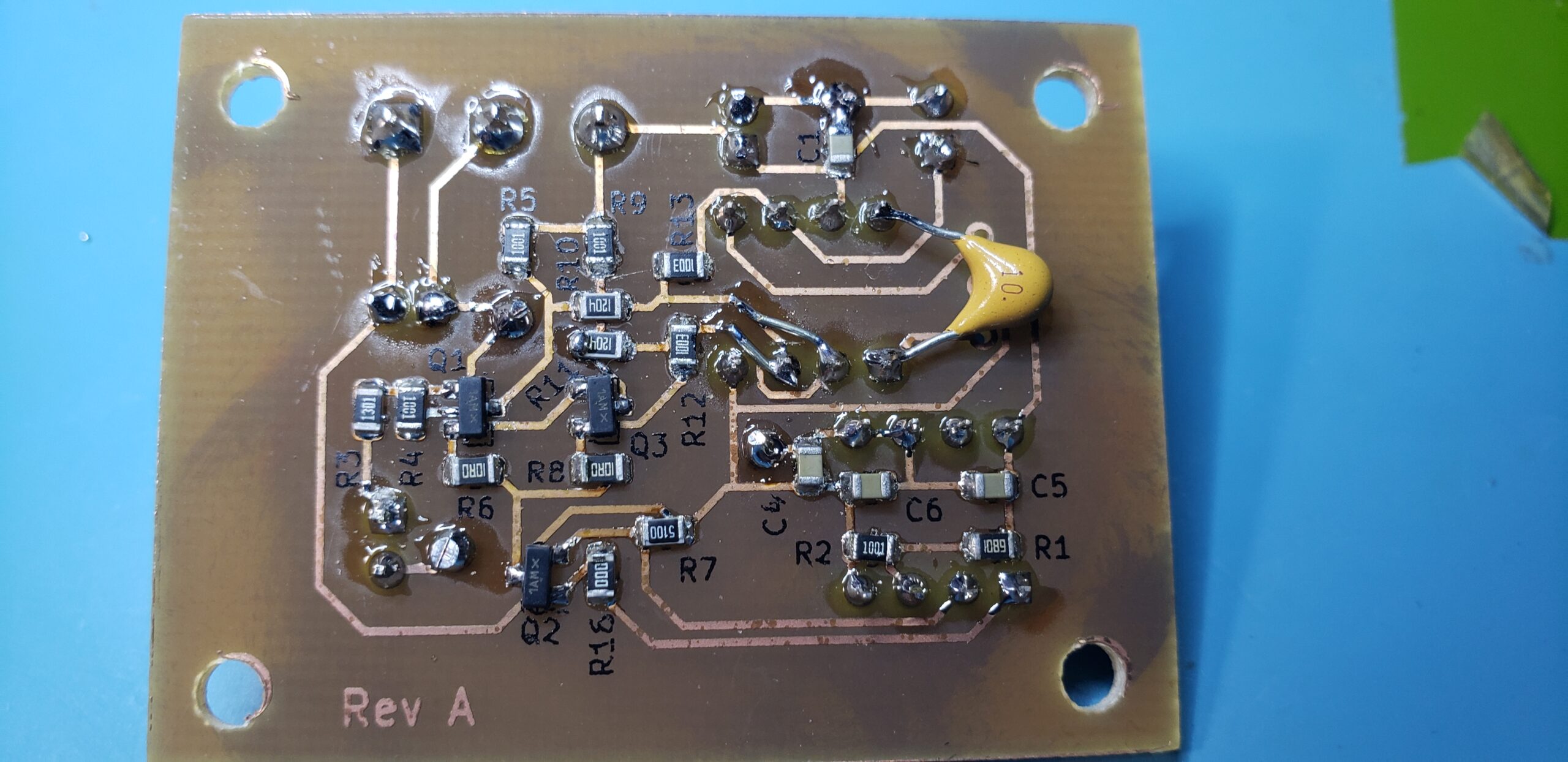
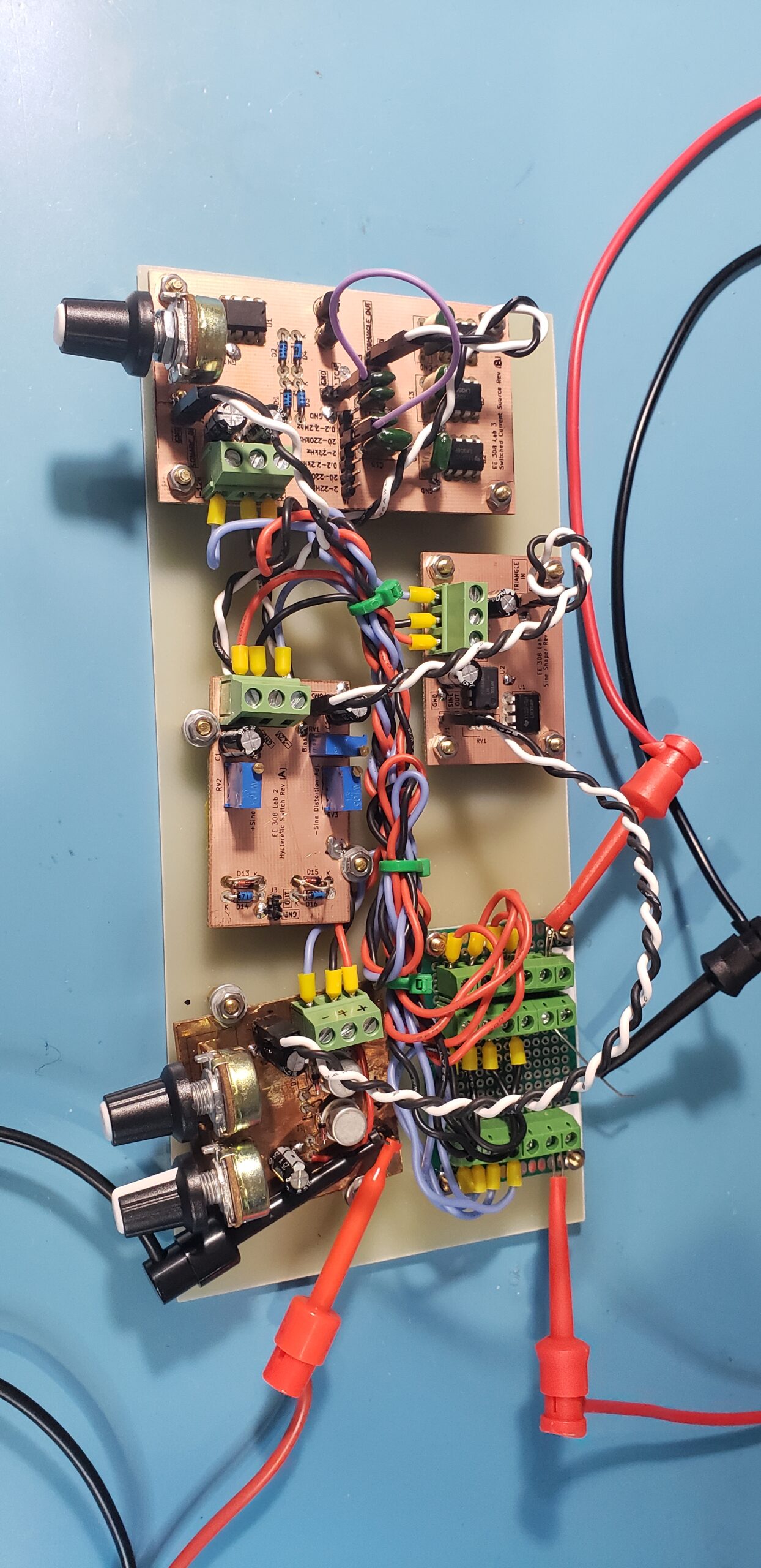
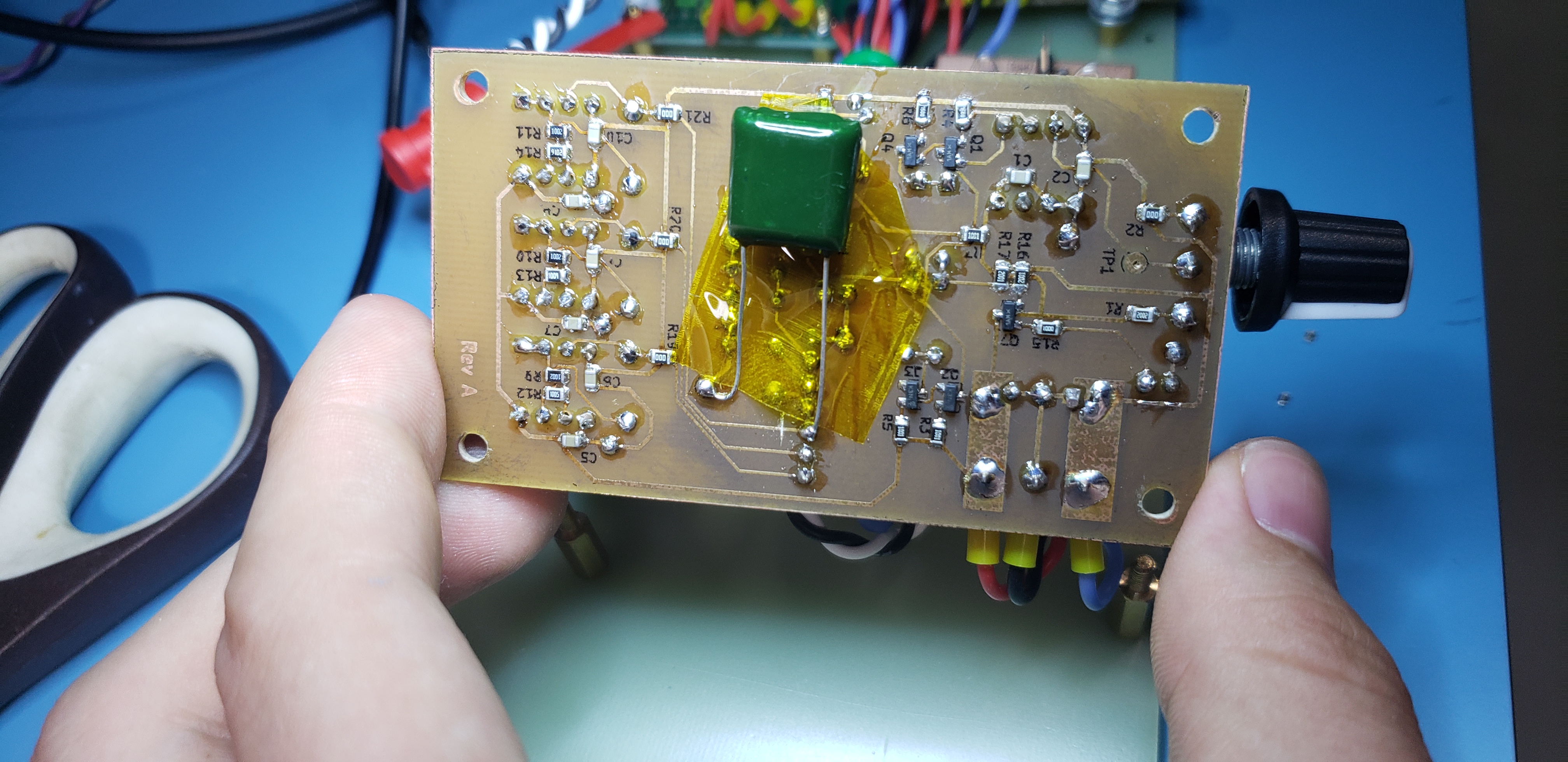
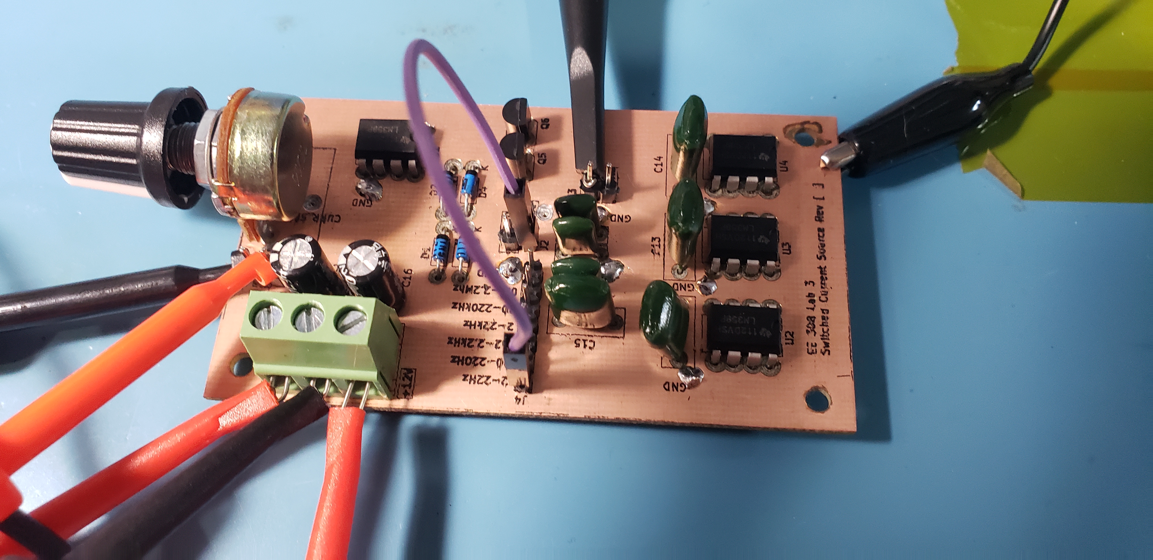
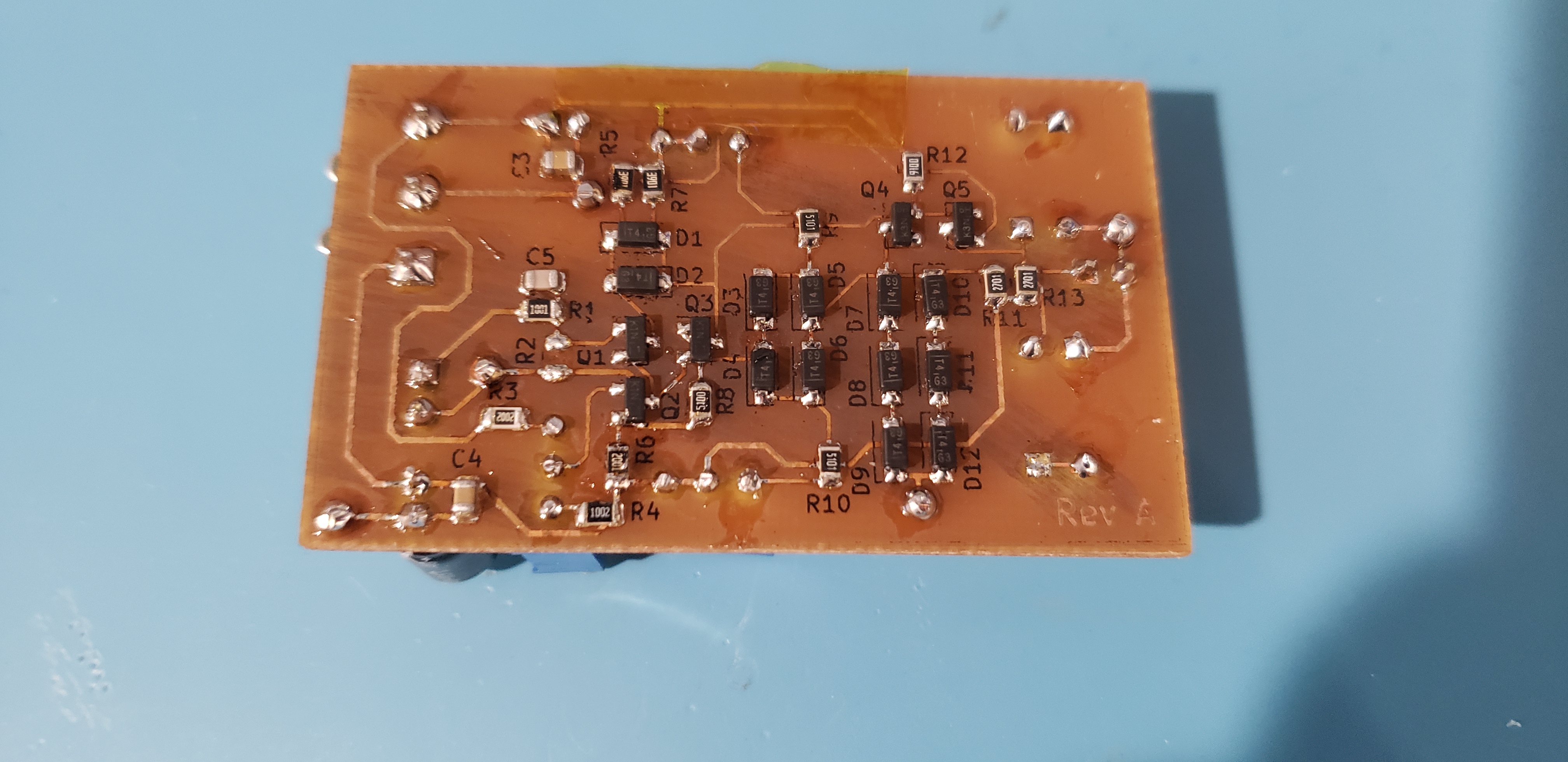
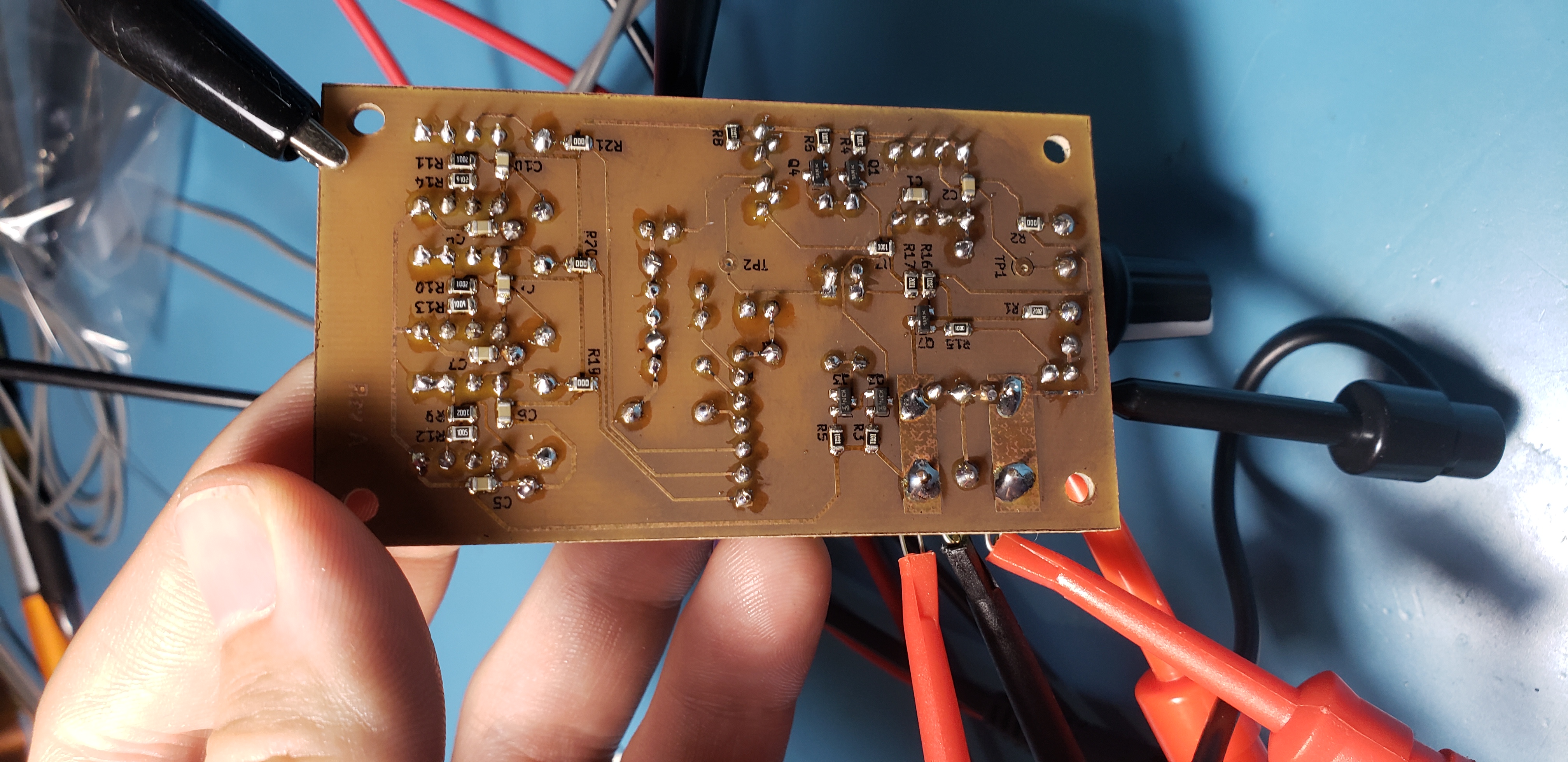
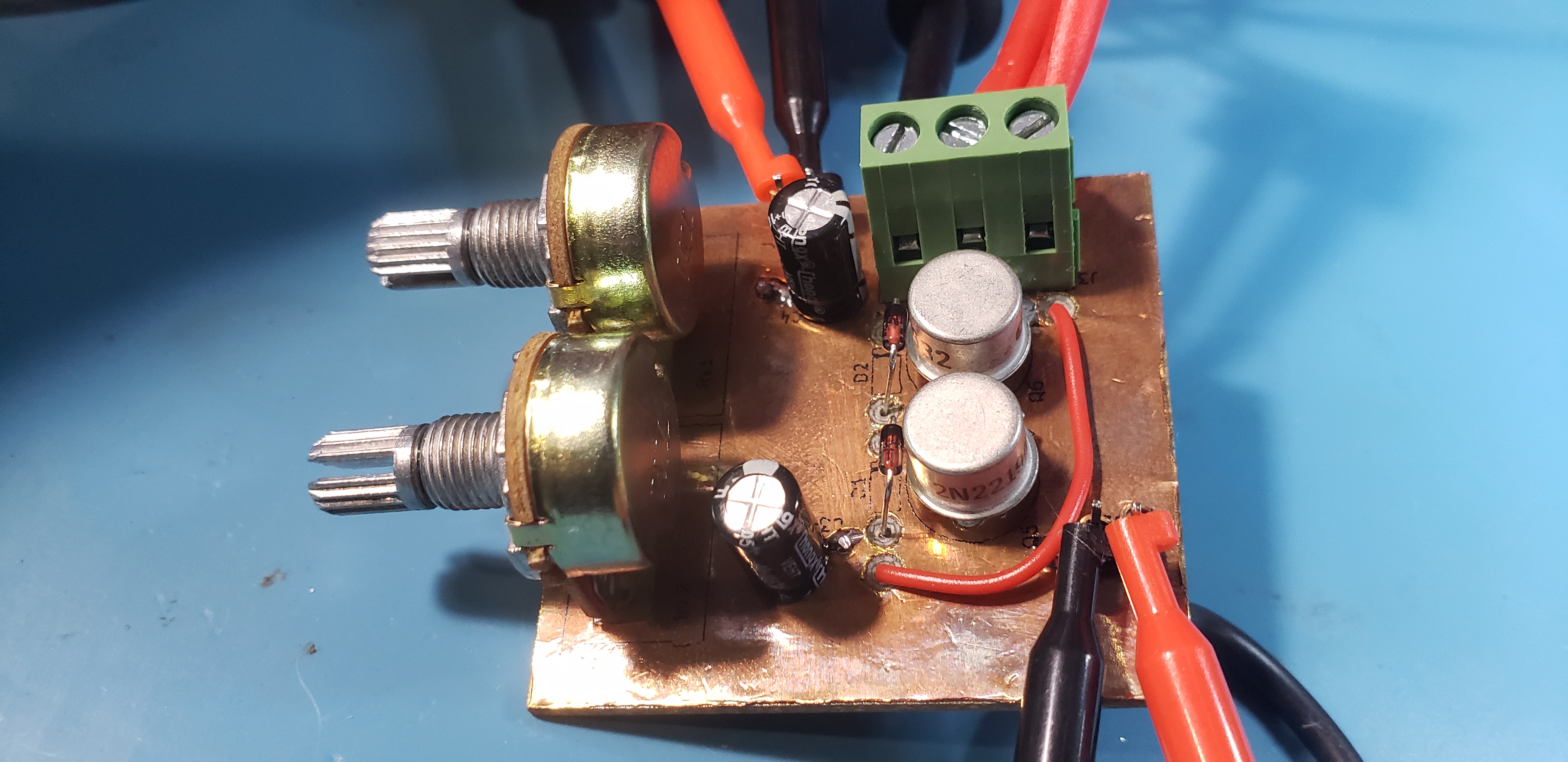
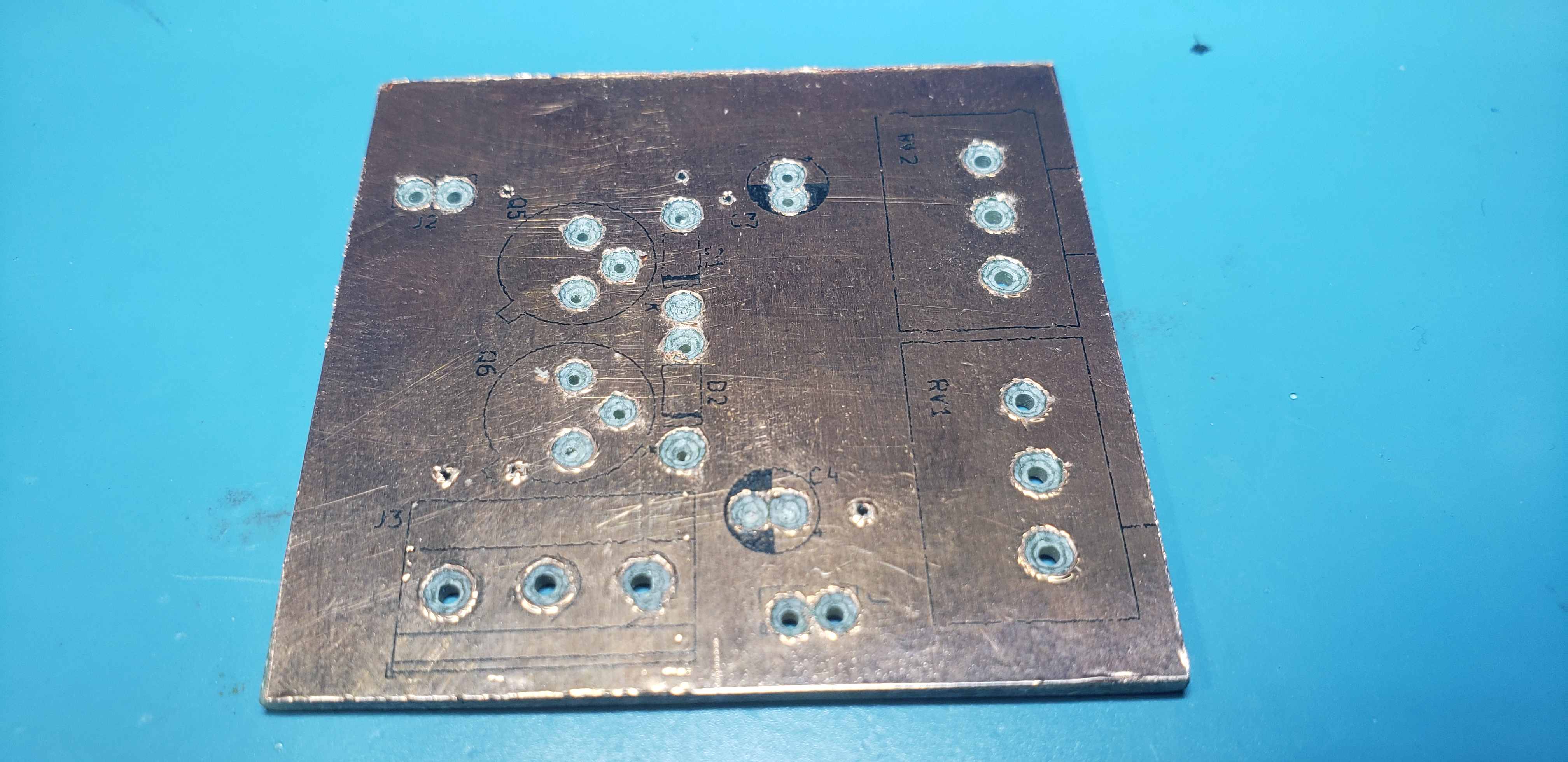
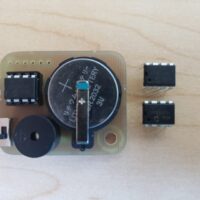
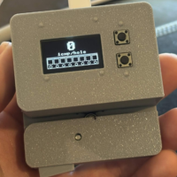
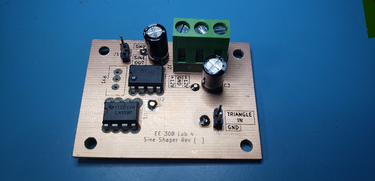
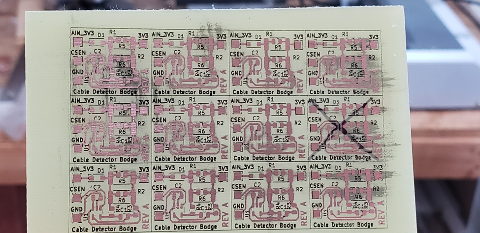
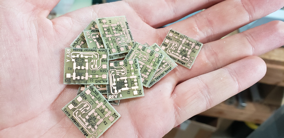
Home-Etched PCB Gallery