I recently came upon design challenge for designing a single-cell battery simulator. I started having a lot of fun with the project–by the time it was done, I figured it was worth documenting as a good example of my hardware and software design workflow. As of the time of writing this post, I’m quite happy with what I made, but I’m hoping that in a few years I can look back at this post in a “look at how far I’ve come!” kinda way. We’ll see! Here’s to learning new things in the future.
The Challenge
The following text in italics is taken from the challenge. Some unimportant details are removed for clarity.
Battery management system (BMS) is one of the critical systems used in electric aircraft to
monitor the status and the health of the battery. To test the performance of the BMS, a battery
simulator is needed.
As shown in the following figure, the designed simulator is controlled by an MCU and it
communicates with a computer via serial communication. The cell voltage can be set from the
computer. The balancing current can be supplied, measured and reported to the computer by
the simulator.
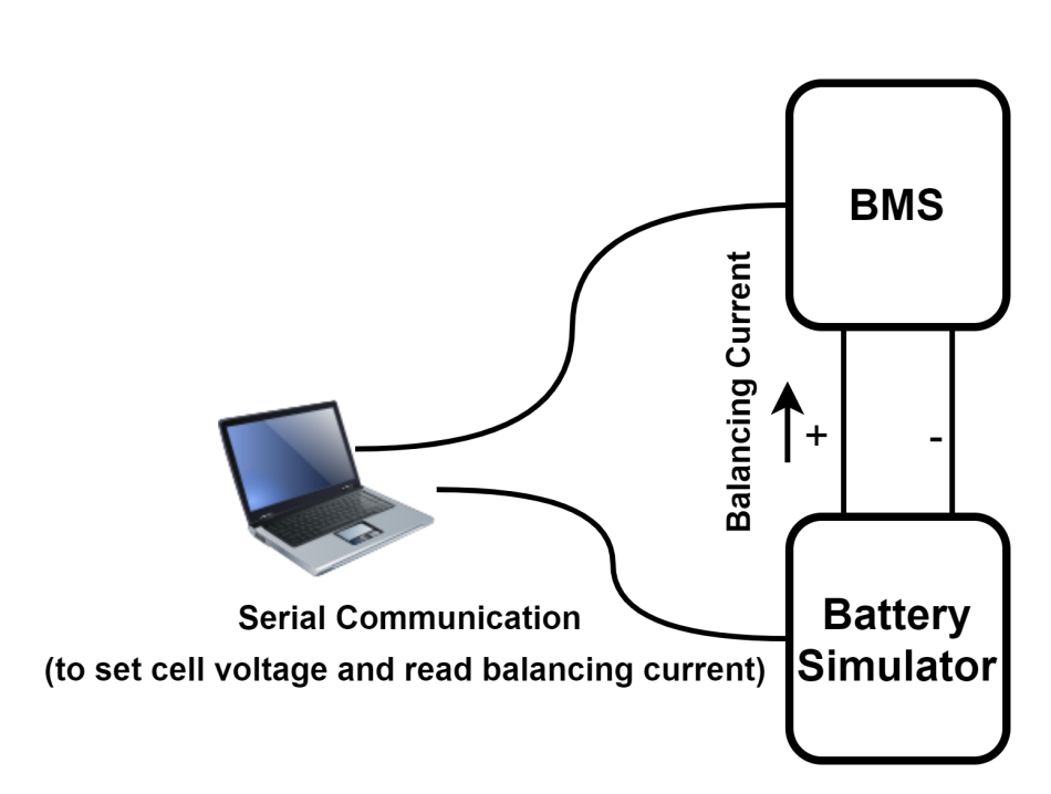
An isolated 5 VDC voltage source is given.
- The cell voltage can be adjusted in the range of 2.5 V to 4.5 V via MCU with tolerance of
±5%. - The simulator can supply and measure the balancing current (current flowing out of the
simulated cell) up to 200 mA with tolerance of ±10%.
What I Made
The challenge really only asked for a rough schematic, but I had a strong hankering for a good analog project and hadn’t touched my op amp drawers for too many months, so I got working on a circuit that I could build with what I had available in the workshop.
After considering various topologies based on linear regulator ICs (not enough headroom) or switching power supplies (didn’t have the chips on hand), I decided that one of the easiest ways to tackle the battery simulator challenge was to build what is essentially a juiced-up op-amp. The circuit would use a generic rail-to-rail op-amp for control, but would drop unwanted voltage from the 5V supply using an external power BJT and an associated drive circuit. While not very energy efficient, this circuit looked like it could be pretty simple and cheap to build, and would meet the relatively modest power requirements of the challenge quite easily. An added bonus was that by using a dual rail-to-rail op amp, I could dedicate the unused op amp circuit to high side current sensing! For compute, I used a Pi PIco since it was readily available, cheap, and I had already built out a docker environment for programming and testing for the RP2040 as a target.
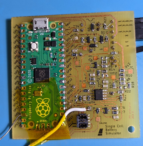
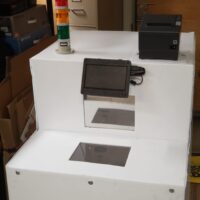
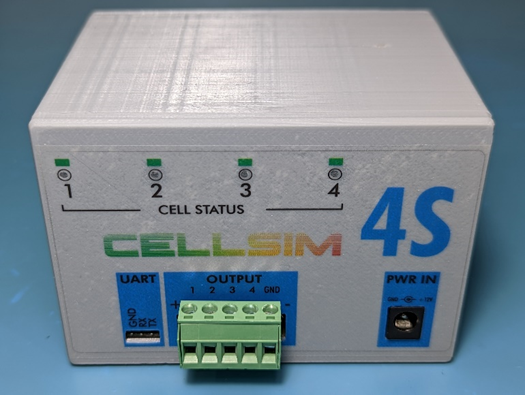
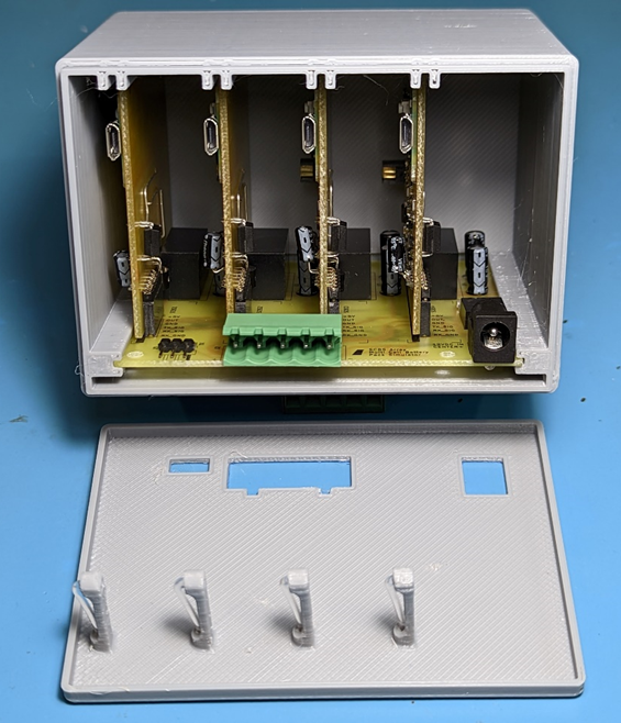
During my design of the battery cell simulator, I added some opto-isolators to allow multiple battery cells to be chained together. I became very curious about whether my design for daisy-chaining cells into a simulated battery pack would work, and decided to build out the motherboard that would allow multiple battery cells to be supplied with isolated 5V power and daisy-chained such that they could communicate with each other and their output voltages would be presented in series. I designed the motherboard such that each of the battery cell circuits could be inserted as a vertical card, and created a 3D-printed enclosure to house the motherboard and all of its installed cards. I bootstrapped an indicator LED for each cell by heat-forming a PMMA optical fiber into a light pipe and affixing one fiber over each Pi Pico’s status LED.
The full design process, stream-of-consciousness debugging and all, is recorded in my design notebook document. Some quick links:
- Design Calculations
- Firmware
- Schematics
- LTSpice Simulations
- Control Scripts
- Mechanical CAD
- Documentation
Datasheets
I documented the completed devices at the multi-cell (Cellsim 4S) and single-cell (SCBS-Pico) levels to capture things before they sublimated from my brain and to dust off the technical documentation skills. There’s something satisfying about writing datasheets!